Digitizing a LVDT Transducer Interface Output

Digitizing transducer interface output voltage is shown on circuit diagram below. The transducer in this case is the NE5521, an LVDT (Linear Variable Differential Transformer) Signal Conditioner. To ensure that the input to the A/D does not go excessively beyond the supply voltage of the A/D, this device is use the diode at the A/D input. For a better description of the operation of the part, you can see the NE5521 data sheet.

Digitizing a Transducer Interface Output circuit schematic diagram

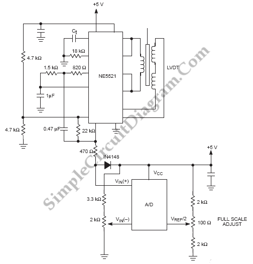
Determine the range of voltages that the transducer interface output will take on to adjust the full scale of the A/D. LVDT core is set for null and the Zero Scale Scale Adjust Potentiometer for a digital output from A/D of 1000 000 is set. The LVDT core for maximum voltage from the interface is set and then the Full Scale Adjust potentiometer is set so the A/D output is just barely 1111 1111. [Source: NXP Application Note]

This entry was posted in Signal Processing, Test and Measurement and tagged . Bookmark the permalink.,

Possibly Related to "Digitizing a LVDT Transducer Interface Output" Circuits

  • Detector for Magnetic Transducer
    Magnetic transducer is usually found in pulse counting application, and we can use this circuit to amplify and convert the signal from the transducer.  Here is the schematic diagram of the signal conditioning circuit: [Source: National Semiconductor Application Note]...
  • AD589-Single Supply LVDT Signal Conditioner Design Procedure
    As well as in dual (symmetric) supply, AD598 LVDT signal conditioning circuit can be configured in single supply operation, here is the schematic diagram of the circuit: The step-by-step procedure to determine the components values for this circuit is available … Continue reading →...
  • AD589-Dual Supply LVDT Signal Conditioner Design Procedure
    LVDT (linear voltage differential transformer) is widely used as linear position sensor.  AD589 integrated circuit provides a complete solution for LVDT signal conditioner circuit. This circuit diagram below shows the connection method with dual +- 15 volt power supplies and … Continue reading →...
  • Voltage To Frequency Converter
    Using this circuit, we can accept positive or negative or differential control voltages. When the control voltage is zero, the output frequency is zero. To charge the timing capacitor C1 linearly, the 741 op amp forms a current source controlled … Continue reading →...
  • Higher Input Or Output for L200 Voltage Regulator
    This is higher input or output for L200 voltage regulator circuit. This circuit is designed to solve the problem that occurs when the input or output voltages are higher than the device can produce. This circuit uses the external components. … Continue reading →...

Comments are closed.