MAX1703 Single-Cell Boost Converter Circuit
When you design a circuit with only a single-cell battery, you will need boost-converter to provide enough voltage for most application. This circuit is a modification of the diode-OR connection circuit. The linear regulator is formed by the U1’s internal gain coupled with the PFET(Q1). The diode-OR connection is connected to Q1’s source that will act as USB power supply. The Q1’s drain can regulate the supply power to 3.3V because the boost-converter’s output is set to 3.4V. Here is the schematic diagram of the circuit:
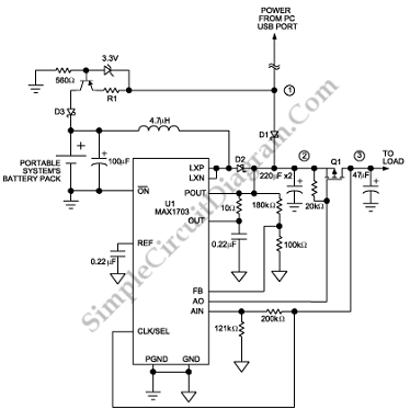
The USB devices require the bus-supply voltage from 4.4V to 5.25V. When the USB devices is connected, the boost converter will idle because the D1 is forward biased. If its output still above the 3.4V regulation point, the boost converter remains idle. The battery is charged by the current source activated by the bus supply. Beside that the bus supply also services the load. The current source current output that is charged to the battery can be set by adjusting the R1.