50V Precision Regulator using LM10 IC
This voltage regulator arrangement is unique, since the op-amp is configured not to see either the source voltage or the output voltage directly, making it possible to regulate higher voltage while the IC is only suffering the transistors bias voltage. Here is the schematic diagram of the circuit:
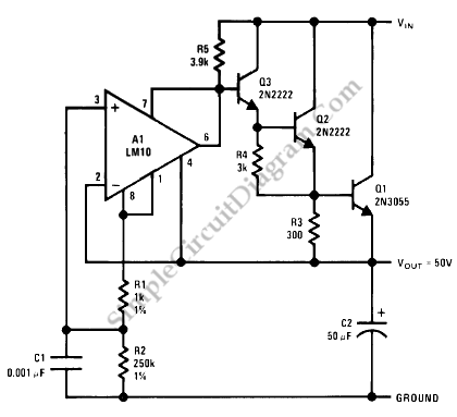
You can see in the diagram that the IC’s power supply pin (7 and 4) is only tied across three transistors base biases. If the current requirement for the output is low, you can replace Q2 with a silicon diode (the emitter of Q3 is connected to Q1 base through a diode). You can’t omit Q2 without replacing with a diode since it will lower the voltage operation of the LM10 IC below its acceptable range.
The principle of regulation is simple, where the op-amp try to null the inverting and noninverting inputs. The noninverting input is supplied with the voltage coming from reference out (pin 1), and it will be initially higher than the noninverting input since the noninverting input is tied to ground of the IC (IC’s v-, where the reference out is referenced). As the result, the output of the LM10 will be open (since it wired as open colector by shorting the output to v+ pin), and the pull-up current won’t be attenuated by the LM10 IC so the transistor will try to pass the current to the full capacity. As the final output voltage is rising, the noninverting input is decreasing since the voltage from the reference is added with the ground of the circuit which is negative relative to the ground of the LM10 (v-). The more voltage the final output the more negative the addition of the reference, and it stop changing when the inverting and the noninverting voltage difference is zero. [Circuit’s schematic diagram source: National Semiconductor Application Note]