The Full-Wave Rectifier and Averaging Filter

The heart of an average reading, rms calibrated AC voltmeter is shown in figure below. It’s a rectifier and averaging filter. We can remove the averaging function and provide a precision full-wave rectifier by deleting C2 and provide an absolute value generator by deleting C1.

The Full Wave Rectifier and Averaging Filter circuit schematic diagram

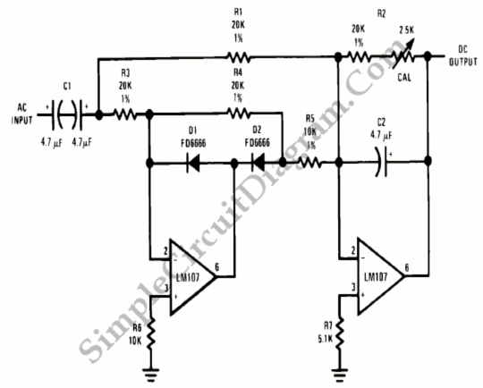
By following the signal path for negative and then for positive input, circuit operation may be understood. The output of amplifier A1 is clamped to +0.7V by D1 and disconnected from the summing point of A2 by D2 for negative signals. A2 then will be behave as a simple unity gain inverter with input resistor,R1, and feedback resistor, R2. This will give positive going output.

A1 operates as a normal amplifier connected to the A2 summing point through resistor R5 for positive inputs. Then amplifier will behave as a simple unity gain inverter with input resistor R3 and feedback resistor R5. Since it is inside the feedback loop, A1 gain accuracy is not affected by D2. Negative current is drawn from A2 summing point through resistor R5 and positive current enters the A2 summing point through resistor R1. The net input current at the A2 summing point is equal to and opposite from the current through R1 and amplifier A2 operates as a summing inverter with unity gain, again giving a positive input since the voltages across R1 and R5 are equal and opposite, and R5 is one half the value of R1.

If the circuit is to used as an absolute value generator, capacitor C1 may be deleted. The circuit output will be the positive absolute value of the input voltage when this is done. For unity gain operation, the amplifiers chosen must be compensated. R6 and R7 must be selected to minimize output errors due to input offset current. [Source: National Semiconductor Application Note]

This entry was posted in Signal Processing and tagged . Bookmark the permalink.,

Possibly Related to "The Full-Wave Rectifier and Averaging Filter" Circuits

  • Op-Amp Circuit: Summing Amplifier
    This is a summing amplifier circuit. This is an inverting circuit that provides an inverted output equal to the sum of all three input. This circuit has some advantages such as there is no interaction between the operation and inputs, … Continue reading →...
  • Wien-Bridge Sine-Wave Oscillator
    This is a Wien-bridge sine-wave oscillator circuit. This circuit uses negative-feedback stabilization to make sure the gain won’t go higher than unity to prevent signal distortion. The D2 and D1 will conduct when Negative peaks in excess of -8.5 V. … Continue reading →...
  • Sine Wave Oscillator
    This is a Sine Wave Oscillator circuit. This circuit as known asĀ  amplitude-stabilized sine-wave oscillator. It can gives high purity sine-wave output down to low frequencies with minimum circuit complexity. This circuit has a several advantages such as it does … Continue reading →...
  • Op-Amp Application: Inverting Amplifier
    The figure below show an operational amplifier circuit. Closed-loop gain given by this circuit is R2/R1 when this ratio is small compared with the amplifier open-loop gain, and it’s called as inverting circuit. The value of input impedance is equal … Continue reading →...
  • Low-, Band-, and High-Pass Single Supply Multiple Feedback Filter
    This is Low-, Band-, and High-Pass Single Supply Multiple Feedback Filter circuit. This circuit uses MFB topology, which has some advantages and disadvantages. The advantages of MFB topology are low cost, easy to implement and very versatile. The disadvantage of … Continue reading →...

Comments are closed.