Analog’s ADP1821 Step Down DC-to-DC Converter
Schematic diagram below shows an ADP1821 Step Down DC-to-DC Converter circuit. This circuit uses ADP1821 that can be used to regulate an output with a load of more than 20 A. It can be done if he power components like MOSFETs, the bulk capacitors and the inductor are chosen carefully to achieve the power requirement. The power-train component limits the power dissipation and the maximum load. To deliver the 20A load, the two low-side MOSFETs are required. Here is schematic diagram of the circuit:
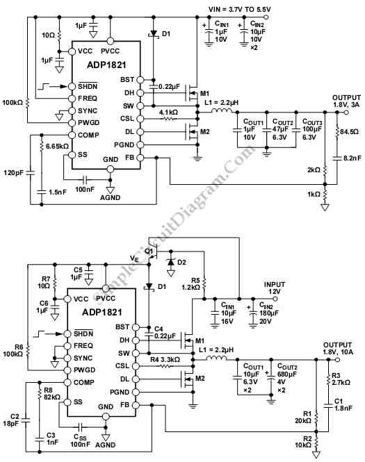
An output load of less than 1A can be driven by The ADP1821. First circuit is a typical application circuit that can drives a 3 A load in an all multilayer ceramic capacitor (MLCC) solution. Two MOSFETs used in this are dual-channel MOSFETs in a PowerPAK® SO-8 package. It can save layout space and reduce the cost.
The ADP1821 can also be used with an input voltage higher than 5.5 V. The second circuit is a typical application circuit that operates from a 12 V input. To power the ADP1821, the input voltage must be stepped down by using external LDO, a 5.6 V Zener diode, a resistor, and an NPN. the LDO that can be used for for input voltages up to 12 V is the ADP3330 or ADP3300. these external signal components are small in size and inexpensive.
The circuit require two power rails, they are a power input rail, with range from 2.5V to 20V and a 5 V bias supply that needs to supply about 30 mA to power the ADP1821 at full load. This circuit uses Sanyo OSCON™ capacitors as bulk output and input capacitors because it has high current ripple rating and low ESR. Aluminum electrolytic capacitors and the polymer aluminum capacitors can used to replace the OSCON capacitors.
If aluminum electrolytic capacitors are used, they must be paralleled up at the input or output to meet the current ripple requirement. To suppress the current ripple and reduce the effective ESR, a larger bulk input and output capacitance is required because the aluminum electrolytic capacitors have much larger variation in capacitance over the operating temperature range and higher ESR. [Circuit’s schematic diagram source: analog.com]