CMOS 4011 Long Delay Timer
A very long time constant is provided by R1 and C1. C1 discharges and the near zero voltage at its positive lead is applied to the high impedance inputs of the four gates of IC1 wired in parallel when P2 is momentarily closed. The battery voltage is available at Q1 Emitter since the four paralleled gate outputs of the IC go therefore to the high state.
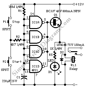
C1 starts charging slowly through R1 when P2 is released and the IC gate outputs fall to zero when the voltage at its positive lead has reached about half the battery voltage, stopping Q1. This transistor can drive a portable radio receiver or different devices directly, drawing a current up to about 250mA. Connecting a Relay across the Emitter of Q1 and negative ground, devices requiring much higher voltage and current operation can be driven through its contacts.
The circuit will start if P2 is pushed for 1 to 5 second and will switch off after about 35 minutes. The time delay can be varied depends on values of R1 and/or C1. If required, P1 will stop the timer. LED D1 is optional. When the load is placed far from the time, LED D1 can be useful to signal relay operation. [Circuit’s schematic diagram source: extremecircuits.net]