Op-Amp Application: Inverting Amplifier
The figure below show an operational amplifier circuit. Closed-loop gain given by this circuit is R2/R1 when this ratio is small compared with the amplifier open-loop gain, and it’s called as inverting circuit. The value of input impedance is equal to R1. Bandwidth of this closed-loop is equal to the unity-gain frequency divided by one plus the closed-loop gain.
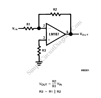
Take a note of this, R3 should be chosen to be equal to the parallel combination of R1 and R2. It’s used to minimize the offset voltage error due to bias current and the offset voltage at the amplifier output and closed-loop gain times the offset voltage at the amplifier input will be equal.
Offset voltage at the input of an operational amplifier consists of two components, input offset voltage and input bias current. For a particular amplifier, the input offset voltage is fixed, however the contribution due to input bias current is dependent on the circuit configuration used. The source resistance for both inputs should be equal for minimum offset voltage at the amplifier input without circuit adjustment. The maximum offset voltage and the voltage drop across the source resistance due to offset current in this case. The prominent error term for high source resistance is caused by the offset current, while the main error for low source resistance is caused by the amplifier offset voltage.
Offset voltage at the amplifier output may be adjusted by adjusting the value of R3 and using the variation in voltage drop across it as an input offset voltage trim in high source resistance application.
Offset voltage is important in AC coupled application but not in amplifier output. Any offset voltage at the output reduces the peak to peak linear output seeing of the amplifier, that’s the only consideration.
To make the oscillation does not occur, the gain frequency characteristic of the amplifier and its feedback network must be such that the phase shift through amplifier and feedback network must be never exceed 180′ for any frequency where the gain of the amplifier and its feedback network is greater than unity, that’s the way how to meet the condition. Since this is the situation of conditional stability, the phase shift should not approach 180′. Obviously the most critical case shows up when the attenuation of the feedback network is zero.
We can use amplifiers which are not internally compensated to achieve increased performance in circuits where feedback network attenuation is high. As an example, since the feedback network has an attenuation of 6 dB, the LM101 may be operated at unity gain in the inverting amplifier circuit with a 15pF compensating capacitor while it requires 30 pF in the non-inverting unity gain connection where the feedback network has zero attenuation. The LM101 slew rate in the inverting unity gain connection will be twice that for the non-inverting connection and the inverting gain of ten connection will yield eleven times the slew rate of the non-inverting unity gain connection since amplifier slew rate dependent on compensation. The trade-off is, stability Vs bandwidth. If we have the stability is rising, we also have the bandwidth is decreasing and vice versa. [Source: National Semiconductor Application Note]