Op-Amp Application: Voltage Comparators

Two reasons why LM101 is well suited to comparator applications are it has a large differential input voltage range and the output is easily clamped to make it compatible with various driver and logic circuits. LM101 doesn’t have the speed of the LM7104 (10us versus 40 ns, under equivalent conditions) but spees is not a problem in many linear applications and the lower input currents along with higher voltage ability of the LM101 is a great benefit. The following circuit diagram show two comparator circuits using the LM101.

Op Amp Application Voltage Comparators circuit schematic diagram

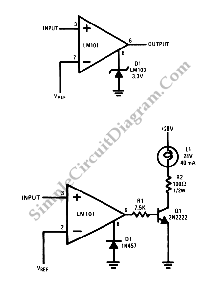
The upper schematic is a clamping scheme which makes the output signal directly compatible with DTL or TTL integrated circuits. The output at 0V or 4V in the low or high states respectively clamped by LM103 breakdown diode. Has a sharp breakdown and low equivalent capacitance are the reasons why this particular diode was chosen. The amplifier operates open loop so normally no frequency amends is needed when working as a comparator. Nonetheless, to prevent low level oscillations when the comparator is in the active region, the stray capacitance between pins 5 and 6 of the amplifier should be minimized. A 3 pF capacitor on the normal compensation terminal will eliminate it if this becomes a problem.

The connection of the LM101 shown in the lower figureĀ  is employed as a comparator and lamp driver. Q1 switches the lamp, with R2 limiting the current surge resulting from switching on a cold lamp. The base drive to Q1 is determined by R1 while D1 keeps the amplifier from putting too much excessive reverse bias on the emitter-base junction of Q1 when it switches off. [Source: National Semiconductor Application Note]

This entry was posted in Signal Processing. Bookmark the permalink.,

Possibly Related to "Op-Amp Application: Voltage Comparators" Circuits

  • Programmable Capacitance Multiplier with DAC
    Capacitance multiplier simulate high capacitance capacitor for analog signal signal processing. By using DAC (Digital-to-Analog Converter), we can simulate variable capacitance with very wide range, which can be used in digitally controlled analog processor (programmable filters for example). The following … Continue reading →...
  • Op-Amp Application: Inverting Amplifier
    The figure below show an operational amplifier circuit. Closed-loop gain given by this circuit is R2/R1 when this ratio is small compared with the amplifier open-loop gain, and it’s called as inverting circuit. The value of input impedance is equal … Continue reading →...
  • Op-Amp Application: Level Shifting Amplifier
    Sometimes, in linear equipment design, it’s necessary to take a voltage which is referred to some dc level and generate an amplified output which is referred to ground. Using a differential amplifier similar to that shown in the circuit diagram … Continue reading →...
  • NPN Transistor Common Collector Amplifier
    This is circuit of NPN Common Collector Amplifier. This circuit can be used for impedance matching. This circuit similar to the Emitter Follower circuit because the emitter of this circuit is follows the base minus a diode drop. This circuit … Continue reading →...
  • Op-Amp Application: Non-Inverting Amplifier
    This is a high input impedance non-inverting circuit. This circuit provides a closed loop gain equal to (R1+R2)/R1. The close-loop 3 dB bandwidth of this circuit equal to the amplifier unity-gain frequency divided by the closed-loop gain. Here is the … Continue reading →...

Comments are closed.