FET Switch: A Voltage-Controlled Analog Switch
This is a JFET switch circuit.This circuit uses a MPF102 JFET transistor. In this circuit, the JFET is symmetrical, so the input can be source or drain. The MPF102 is used because this transistor has gate’s reverse breakdown voltage of greater than 25 and in order DSG. The supply of this circuit is ±12V since the maximum gate’s reverse breakdown voltage is 24V. This circuit has two state,ON state and OFF state. Here is the schematic diagram of the circuit:
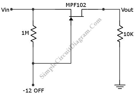
In the OFF state, the gate voltage is -12V and the JFET will off for full signal range because the pinchoff voltage of MPF102 is less than 8V. When the voltage is grater than 8V, the JFET will become ON stage and then gate and source will be connected by 1M resistor. This connection will give a zero bias. Be carefull, the damage can be occured when the gate become foward biased or the drain too positive to the source. To get the ON resistance of the JFET, the output and input voltage must be measured. For the 10K load and 5V signal voltage, the ON resistance is 167R.