NPN Transistor Common Collector Amplifier
This is circuit of NPN Common Collector Amplifier. This circuit can be used for impedance matching. This circuit similar to the Emitter Follower circuit because the emitter of this circuit is follows the base minus a diode drop. This circuit has voltage gain of one because the output voltage is forced to follow about 0.6V below the signal input. Here is the schematic diagram of the circuit: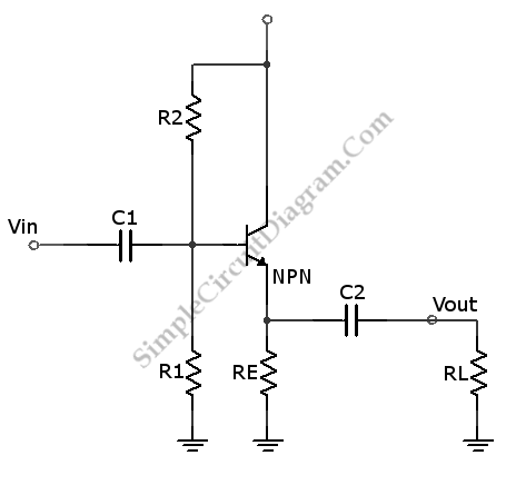
The input impedance is primarily determined by R1 and R2 (in parallel equivalence), since the effect of output impedance to input impedance is attenuated by factor of transistor’s gain. For example if RE in parallel with RL is equivalent to 10k, and hfe=100, then the input impedance contribute by this output impedance is 1M, high enough to be neglected if we use R1 and R2 in a range of 10k-100k.