Low Drift Sample and Hold
This is a circuit of low drift sample and hold. This circuit uses two JFET, Q1 and Q2 that provides the sample and hold capacitor, C1. Q1 provides a path, Rds(on), for C1 and turned on during sample. Q2 IGSS (<100 pA) and Q1 ID(OFF) (<50 pA) as the only discharge paths because Q1 is turned off, during hold. Here is the circuit :
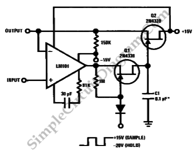
Output current and feedback to the LM101 are supplied because Q2 serves a buffering function. [Source: National Semiconductor Application Note]