Op-Amp Application: Level Shifting Amplifier
Sometimes, in linear equipment design, it’s necessary to take a voltage which is referred to some dc level and generate an amplified output which is referred to ground. Using a differential amplifier similar to that shown in the circuit diagram below (the upper one) is the most straight-forward way of doing this. However, this circuit has a disadvantage, that is the signal source is loaded by current from the input divider, R3 and R4, and to prevent erroneous outputs from the common mode input signal the feedback resistor must be very well matched.
The other circuit diagram below (the lower circuit) doesn’t have the problems mentioned above. A voltage drop across the feedback resistor (R1) is generated by an FET transistor on the output of the operational amplifier which is the magnitude is equal to the input voltage. Here’s the circuit diagram:
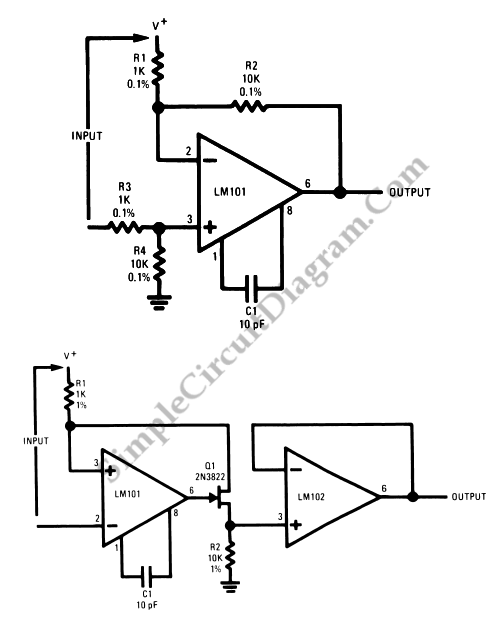
The input voltage multiplied by the ratio R2/R1 will be equal to the voltage across R2; and the common mode rejection will be as well as the amplifier basic rejection, independent of the resistor tolerances. LM102 voltage follower buffer this voltage to give a low impedance output.
The capability work with input voltages up to it’s positive supply voltages as long as the supplies are less than +- 15V is the advantage of LM101 in this circuit. [Source: National Semiconductor Application Note]