Variable Voltage Reference
A positive variable voltage reference circuit is shown in the schematic diagram below. A voltage reference can be made using a zener diode, but this method produce a fix reference value. To make a variable reference, we can amplify the fix voltage reference using active components (op-amp or transistors). Here is the schematic diagram of the circuit:
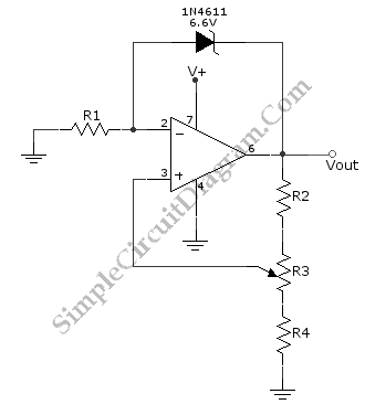
This voltage reference circuit design has unique configuration, where a zener diode is inserted in the negative feedback loop. The basic operation principle of this circuit is the self-stabilization of negative feedback system. We can simplify the stabilization mechanism by a simple rule that the op-amp will produce an output to null the difference between the inverting and non-inverting input’s voltage. Practically it’s true since the circuit must produce a certain level that must be produced by a very small difference between the inverting and non inverting input, as the output of any op-amp in non saturated condition should equal to the difference times the open loop gain which is very large (generally more that 10000).
Output Voltage Formula
The voltage level of this circuit’s output is equal to the zener’s voltage + R1 voltage, where R1 voltage is equal to the current times the resistance. The current flow through R1 will be equal to the current flow through diode, since we can assume the op-amp input pin draw very small current (theop-amp’s input impedance is very high). So, we write the first formula:
[eq.1] >> 6.6V+ IR1 = Vout
The voltage at R1, i.e. IR1, is the voltage level at inverting input Vinv, we ca formulate:
[eq.2] >> Vinv= IR1
At the non-inverting input, the voltage is equal to the output voltage times the voltage divider factor. This voltage level is also equal to the inverting input by the means of regulation mechanism that try to null the difference. We can express this situation as:
[eq.3] >> Vinv = ((R4 + R3′) /(R2+R3+R4)) Vout,
where R3′ is the part of the used resistance that is set between center tap and R4 connection.
Finally, form all equations [eq.1], [eq. 2], and [eq.3], we can deduce the final formula:
6.6V+[(R4 + R3′) /(R2+R3+R4)] Vout = Vout;
[(R4 + R3′) /(R2+R3+R4)]Vout – Vout = 6.6V
{[(R4 + R3′) /(R2+R3+R4)] -1}Vout = 6.6V
Vout=6.6V/{[(R4 + R3′) /(R2+R3+R4)] -1}
You can select the resistor values to get the desired voltage adjustment range, but consider that at any operating point:
- The current flowing through R2, R3, and R4 should not cause excessive power dissipation.
- The current flow through R1 and the diode should not cause excessive power dissipation, and the current variation should fall within the best diode regulation (see the diode’s current versus forward voltage bias).
You can use a standard 5.6V zener diode if you find difficult getting the specified 6.6V one. Other diode values is not recommended since they’re usually has worse stabilization figure (they doesn’t has sharp I-V curve). The op-amp should be selected to cover the voltage swing of the output, and the current handling should be able to handle the current flowing to the load, the R2, and to the diode. That’s all the general consideration in selecting proper component values for this voltage reference circuit design. Have a great experiment with circuit!